Tuesday 30 May 2017

The ESP8266 Alarm Can Now Send Emails

Here's the result:

An email alert as seen in my inbox:

The code is here. The credentials and recipient email address are defined in email.h at the moment, so changing settings requires a reflashing at the moment.

The ESP8266 does a DNS lookup for gmail's SMTP servers, then connects with SSL, logs into an email address I set up specifically for this device and sends off an email. I have only tested this with gmail, where I enabled the option to allow "less secure apps" and also created an app-specific password (I don't know if other email services provide this) - which is a necessary precaution, as I haven't implemented certificate verification yet.

If you ever want/need to debug SMTP over TLS/SSL, as I had to do a lot of, here's a useful command to run on Linux if you have OpenSSL installed (you most likely do):

openssl s_client -crlf -connect <server>:<port>

It lets you talk directly to the server in plaintext from a terminal, just as if you were using a telnet terminal to talk over an unencrypted connection. The only thing to note is, do not send the character 'R' as the OpenSSL terminal intercepts this and interprets it as a command to renegotiate. This caught me up for a long time when I was trying to send "RCPT TO: ..." as you do for SMTP; lowercase is a better choice it seems.

Here's a screenshot of sending an email with SMTP, as I thought would be a good idea to figure out how to do by hand before implementing it on the ESP8266. The lines with numbers 1-7 are steps/commands that I sent. The authentication string (step 2) is just the username concatenated with the password, all encoded in base 64.

Some additions to the web page interface: 

The page now looks like this before any sensors are triggered:


The additions are the new options to arm/disarm the alarm and time stamping. Pressing these buttons achieves the same thing as pressing the wireless key fob which came with the original alarm base station, which this alarm system now listens for.

After some sensors have been detected:

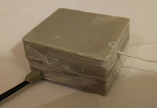
 A printed case:

"But it looked alright on the computer"

Definitely only a first revision enclosure. I designed it a bit small, with walls too thin as well, so it doesn't quite close properly, and the overlap/interlocking bits are tiny (can't really see them in the photos).
Also - oops: I tried polishing the printed plastic with an ABS plastic and acetone solvent solution... but it was white ABS dissolved in the acetone.

Conclusion:

In all, seemed like it would be an easy feature to add; SMTP is simple after all, but to get this one working reliably was a challenge with the complexity of needing SSL on the ESP8266. So if you are looking to get SSL working on the ESP8266 and need more working examples take a look at the code.

Wednesday 17 May 2017

Engraving a Prototype PCB

I put the CNC engraver to use milling a prototype single-sided PCB for the ESP8266 alarm system I've been working on. The tutorials on the internet for PCB2Gcode and KiCAD were pretty easy to follow, so this post is not a tutorial, but just for documenting my experience and some gotchas.

Design

The final design of the board in KiCAD


The board is a connector board really. It powers the ESP8266 module at 3.3v and the 433MHz module at 5v, pulls up the reset and CH_PD pins on the ESP8266 and the buttons allow it to be easily reset and programmed (there's a UART header on the board too). For the wireless alarm system side of things it has a connector for the 433MHz wireless module to plug into, the output of which is voltage divided to get it down from 5v to somewhere in the neighbourhood of 3.3v, which the ESP8266 can handle.

Toolpath generation

Converting the Gerber and drill files from KiCAD into G-code instructions with PCB2Gcode. 
You always have to watch out for potential issues with mirroring at this point in the process, otherwise you might mill and drill a PCB only to find it "off" somehow. That reminds me of an early trap I ran into in KiCAD of the SMD component pads being on the opposite side of the board to the traces. This of course makes no sense for a single sided board without vias. The side that traces and SMD footprints are on can be changed, however.

The drill files were a bit of a nightmare because this PCB needed about five different drill sizes ( which I have), but it means lots of tool changes. The G-code that PCB2Gcode outputs also seems to expect your machine to be capable of automatic tool changes, which mine cannot do. I got around this by manually separating the G-code for each drill size into its own program. I'll have to look into writing a script to do this for me and/or insert a pause command into the G-code, if the feature does not already exist in PCB2Gcode.

It's important that Grbl doesn't have its position zeroed out between programs or it'll make a mess of things. Alternatively, and to be on the safe side, have the machine return to (0,0,0) position at the end of each file and don't do any homing, just so you always have a reference point.

Engraving/Milling


The tooling that was used. None of the tiny little drills were broken, to great surprise. The v bits on the other hand are made of a fair hunk of carbide and are really tough - I accidentally cut the board outline in a single pass (~1.2mm cut depth) and there weren't any issues.

The CNC engraving setup with the board in the process of being engraved.
The finished board.
The clamps holding the board down were scarily easy to undo after all the vibration of cutting; I'll have to put spring washers under the bolts to stop them coming loose. If the board had come loose in the middle of cutting I would have had to start over again without any way to align the board to the bed.
Even more closeup. Not all traces have been fully isolated, and some have too much taken off. The board must not have been completely flat and level, and I think the settings have underestimated the dimensions of the cutting bit.
A bit more tuning of the settings in PCB2Gcode will be needed, and probably also a program which probes the surface of the board before cutting to determine where the surface of the board is, so that a constant cutting depth can be achieved.

The populated board. The ESP-01 breakout board is socketed (can't be seen from this angle).

EEEEKKK! Not nice soldering. I blame the lack of soldermask and the pads coming out undersized - did not make for very forgiving conditions. There's also one bodge wire, for a trace that was completely wiped out; it isn't very easy to make out in the photo however.

Assembled and ready for programming.
There's a 0.1mm copper wire soldered (and secured with a blob of hot glue) onto the actual QFN package of the ESP8266 to get access to an additional GPIO pin because the ESP-01 board does not break out enough free GPIO. This was actually factored into the design, so the board I designed has a pad which the other end of the jumper lead is soldered onto.

More to come on the ESP8266 wireless alarm system soon...